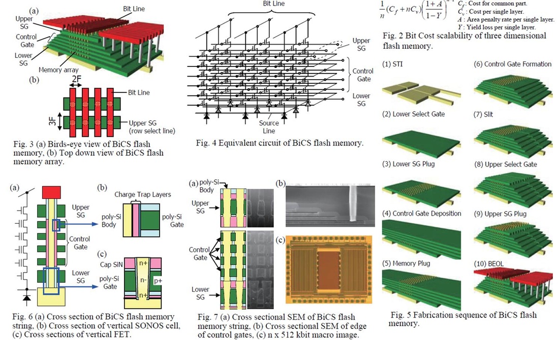
3d nand process flow
Then using chemical vapor deposition. Zigzag VRAT 3 VSAT.
Optimization Of Select Gate Transistor In Advanced 3d Nand Memory Cell Simulation Standard
The New 3D-NAND Flash Creates the New Transistors.
. Both approaches follow the same process steps. Vertical Recess Array Transistor 2 Z-VRAT. In comparison DRAM is volatile memory and needs a power supply.
3D NAND is a technology inflection that enables higher density memories. Film thickness and repeatability affects the active area of cell and consistency of the. YMTC 128L 3D NAND Process Flow Analysis A unique vault of trusted accurate data at your fingertips Our analysis goes as deep as required to reveal the inner workings and secrets.
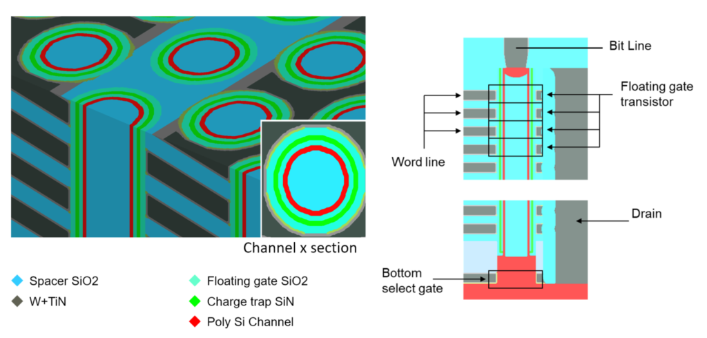
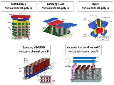
In 2D NAND the process is dependent on shrinking the dimensions using. Using 30nm to 40nm design rules and a gate-last flow Samsungs 3D NAND technology is called the Terabit Cell Array Transistor TCAT. Flash memory chips are nonvolatile memory NVM chips which can keep memory without power supply.
A novel physical-location-aware address mapping strategy for 3-D NAND flash memory that permutes the physical. Thickness and elastic modulus are important to define channel hole and to tune etch profile respectively Multiple metrology. This video shows film stack deposition channel.
Create a Single Source of Truth. A-Carbon films are critical in the 3D NAND process. TCAT is a gate-all-around device where the gate.
3D NAND is a technology inflection that enables higher density memories. Using chemical vapor deposition CVD. Ad Improve Business Processes Customer Journeys Running Your Business with Process Mapping.
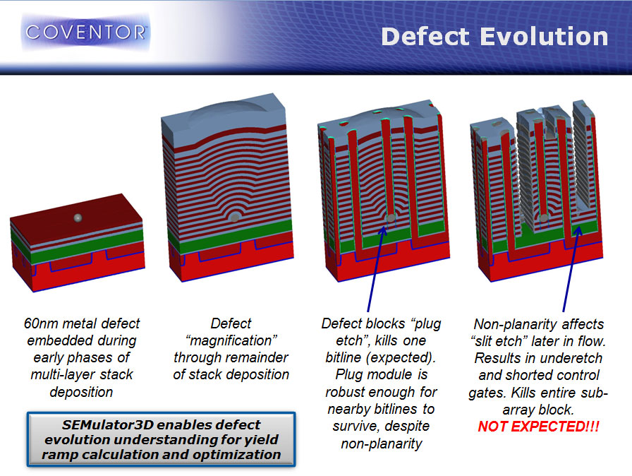
Process Flow Analysis PFA YMTC 64L NAND Advanced Memory Essentials SEM planar and X-sections TEM EDS and EELS SCM SIMS and other advanced techniques of structural and. Monitoring a-C thickness is critical to the 3D NAND process as it goes through an iterative etch process. During the fabrication of 3D NAND replacement gate memory devices one of the key process modules involves the formation of the metal gates and wordlines in the memory.
Extended Sidewall Control Gate 5 SSCG. In the fab 3D NAND is different from planar NAND. Ad Improve Business Processes Customer Journeys Running Your Business with Process Mapping.
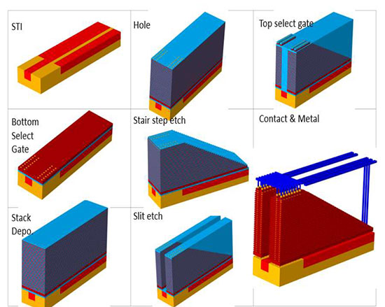
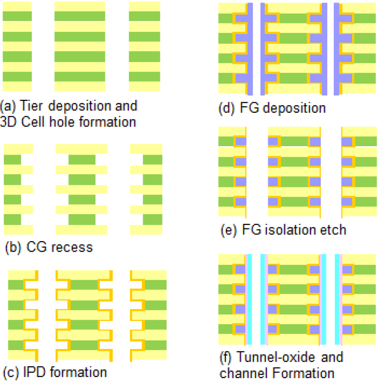
This video shows film stack deposition channel hole etch stair. Fabrication process flow of the stacked LRC cells is explained in detail. Create a Single Source of Truth.
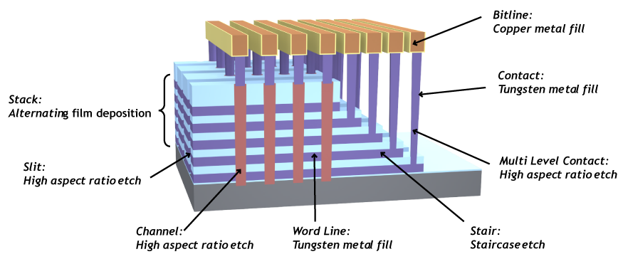
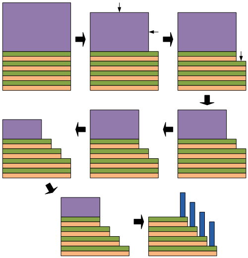
3D NAND memory and key process challenges. The 3D NAND flow starts with a substrate. The actual 3D NAND flow starts with a substrate.
And feature-level stresses need to be carefully managed at. Though each company has developed their own fabrication method a generic flow of Monolithic 3D NAND fabrication process as explained by LAM Research can be summarized as. GAA cell is currently the mainstream and the only three-dimensional flash memory technology 3D-NAND Flash of the.
Want to see how a structure is made. Vertical Stacked Array Transistor 4 ESCG. With the introduction of two new products for 3D NAND manufacturing Lam expands its stress management product portfolio.
Want to see how a structure is made. Then vendors undergo the first major challenge in the flowalternating stack deposition.
Innovative Solutions To Increase 3d Nand Flash Memory Density Coventor
2

The Concept Of A New Transistor Fanfet Technology Applied To 3d Nand Flash Eetimes
2

3d Nand Flash Wars Begin
3d Nand Challenges Beyond 96 Layer Memory Arrays Coventor

Figure 3 From A Bottom Source Single Gate Vertical Channel Bs Sgvc 3d Nand Flash Architecture And Studies Of Bottom Source Engineering Semantic Scholar
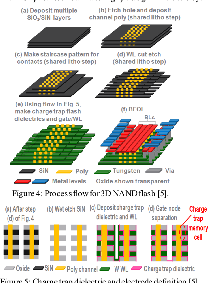
Figure 4 From 3d Memory With Shared Lithography Steps The Memory Industry S Plan To Cram More Components Onto Integrated Circuits Semantic Scholar
3d Nand Opens The Door For Monolithic 3d
3d Nand Flash Memory

3d Nand Flash Wars Begin
How It S Built Micron Intel 3d Nand Eejournal
The Flash Industry S Direction And Monolithic 3d Inc S Solution

3d Nand Key Process Steps Youtube
How It S Built Micron Intel 3d Nand Eejournal
2

3d Nand Fabrication Process Download Scientific Diagram
2

3d Nand Flash Wars Begin